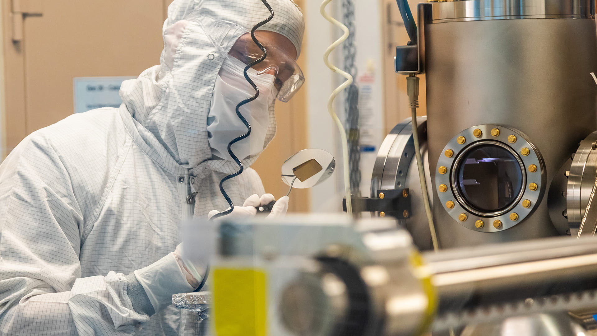
Semiconductor foundry
Raw materials are designed and built from the atomic level into microchips called MMICs.
At temperatures reaching 1,300 degrees Fahrenheit – hot enough to melt rocks into lava – the machine then shoots single atoms of those elements onto a circular wafer. The atoms settle into place, and, layer by layer, they form a crystal-like semiconductor substrate.
Building that substrate is the first step in manufacturing a microchip – the basic building block of electronic devices from cellphones to x-ray machines.
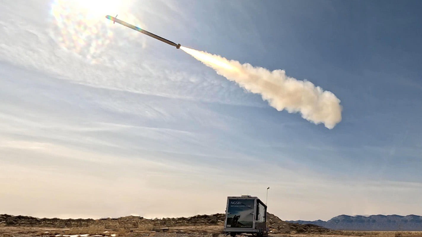
But these microchips, designed by Raytheon’s Advanced Technology business in Andover, Massachusetts, aren’t going into just any electronics. They’re going into powerful military radars that will one day look into sky and space in search of incoming missiles and adversary aircraft.
Those systems, including the Lower Tier Air and Missile Defense Sensor, Patriot, SPY-6 and TPY-2 radars, are produced at the same campus – making Andover a place where radars come to life, from the atomic level through production and testing.
“We’re able to design, lay out and build our transistors and circuits, and tailor them for our systems so that they can have the best performance possible,” said Matt Tyhach, who leads the next-generation sensor development team for Raytheon Advanced Technology, which researches and develops new technologies and products that can be used to upgrade or create capabilities across RTX.
“There’s no compromise in terms of getting our warfighters the best capability possible to win on the battlefield.”
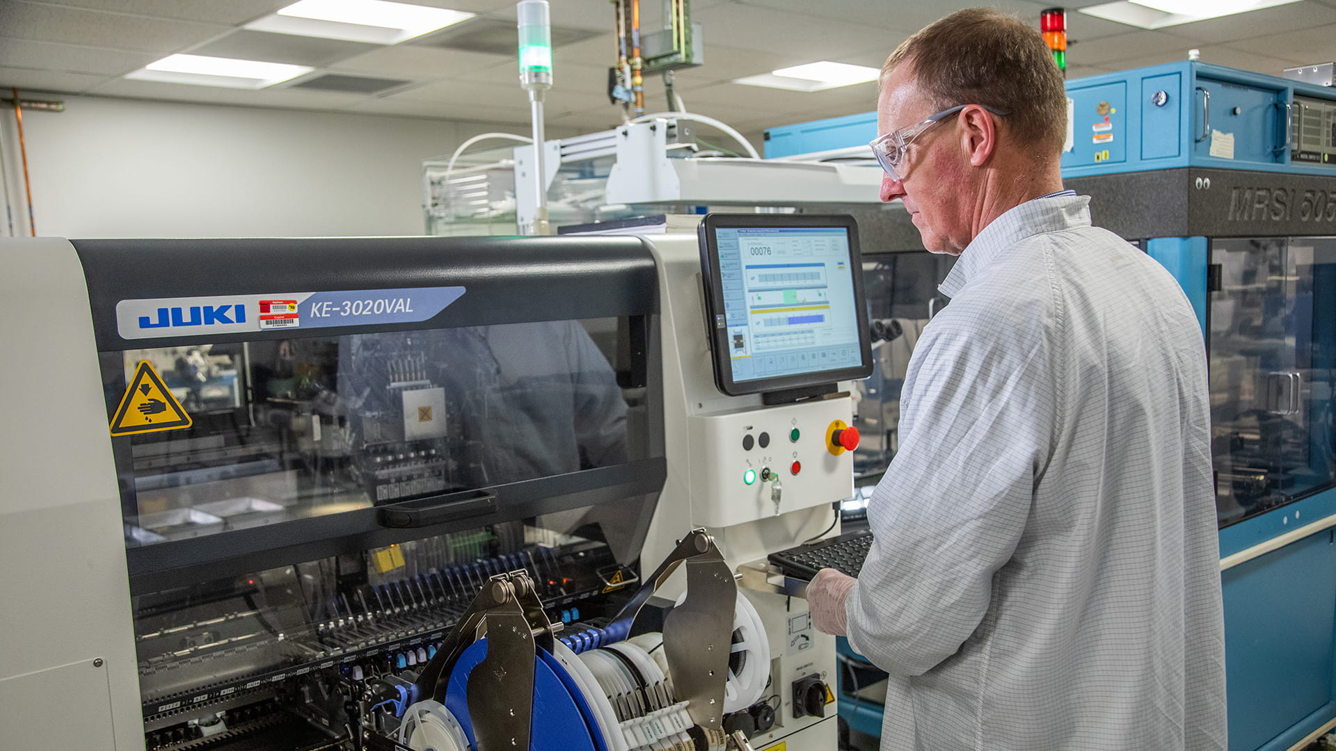
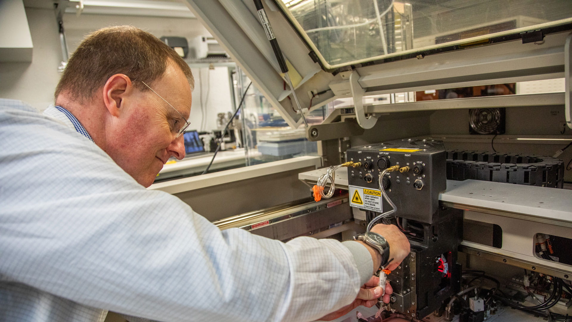
It’s unusual for one facility to perform every step of a manufacturing process, but Raytheon’s radar production site in Andover, Mass., does exactly that. The result: RTX works faster and more affordably to deliver products built to their customers’ needs.
Amanda Kirchner, who manages operations for RF technologies in Andover, said she thinks of the campus as several individual manufacturing businesses whose products come together to make one final product. Hear her explain how Andover’s design streamlines and improves manufacturing.
In her words
Radars begin in Andover’s foundry, where teams design radio frequency power amplifiers, which boost a radar’s signal. With stronger signals, radio waves travel farther and return with higher-fidelity information about the target.
One of Raytheon Advanced Technology’s major advancements was a new semiconductor design based on military-grade gallium nitride. Gallium nitride, known as GaN, provides three to five times better performance than the previous leading semiconductor, gallium arsenide. GaN packs more power into a smaller footprint, clearing the way for new radars on aircraft and other platforms with strict space and weight constraints. Additionally, the advancement made possible Raytheon’s software-defined aperture approach, a radar architecture that allows for secure and flexible software upgrades and faster development to meet customer demand.
“It also benefits scanning and sensitivity – the volume that can be searched in the same timeframe. That’s important for missions that are constantly scanning the skies for threats like cruise missiles, ballistic missiles, etc.,” Tyhach said. “GaN really breaks apart some of the fundamental limits of physics.”
Raytheon began investing in GaN in the early 2000s, beginning with the use of the molecular beam epitaxy tool and eventually making its way through development and production of the SPY-6 radar, which Tyhach describes as the “workhorse” of the U.S. Navy’s fleet.
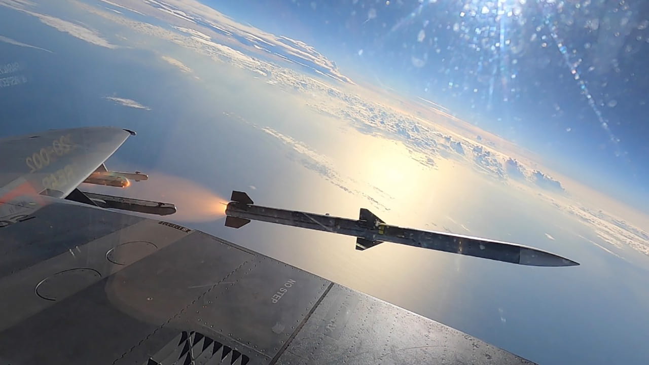
GaN has made its way into multiple products since then, including the Patriot Air and Missile Defense System, the Next Generation Jammer for fighter jets, and the U.S. Army’s Lower Tier Air and Missile Defense Sensor.
The system, a 360-degree radar often called LTAMDS, recently went into production after rigorous field testing. That testing started with a working prototype built in less than 18 months – a process that would normally take years.
“For us to basically cut the amount of time in half and meet the deadline was a significant achievement,” said Chris MacDonald, a senior technical fellow in Andover’s foundry who focuses on semiconductor development.


While their work with GaN was a great success, Raytheon Advanced Technology is always thinking about what’s next. Along with the Defense Advanced Research Projects Agency, they’re exploring how to pair GaN with other materials like diamond to manage heat and looking at new semiconductor materials like aluminum nitride that will one day unlock new possibilities like GaN did.
“How do we get more power per element out of our systems to offer new breakthrough performances?” Tyhach said. “I spent the first 10 years of my career here as an RF designer, so I certainly appreciate the full process, and really the symphony that it takes for one of these designs to be made and then ultimately fielded into one of our systems. It’s an incredible feeling when you know that your work is making a difference, whether it’s for the United States or across the globe.”